
 Download:
Figures of the Article
-
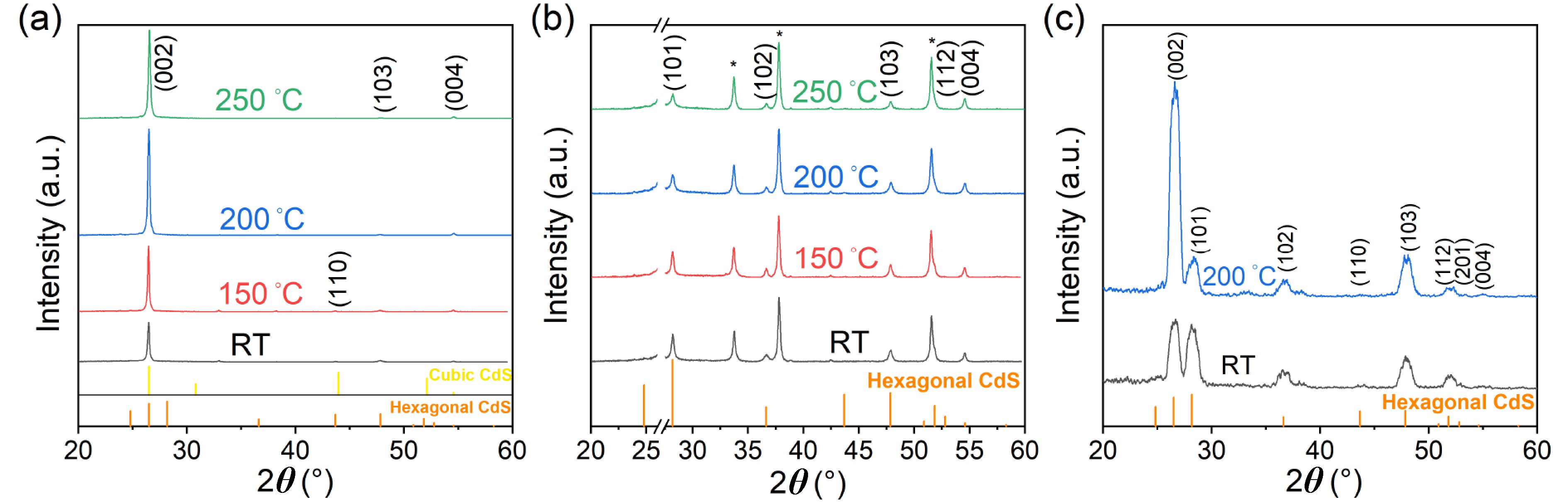
![]() X-ray diffraction (XRD) pattern of the sputtered CdS thin film. The deposition time was 2 h, four times the standard CdS growth time. (a) CdS sputtered on a glass substrate at different temperatures. (b) CdS sputtered on an FTO substrate. The positions of the FTO diffraction peaks are labeled with asterisks. (c) Grazing incidence XRD (GIXRD) result of CdS sputtered on an FTO substrate. The incident angle is 0.4°, and no FTO substrate peaks are found.
X-ray diffraction (XRD) pattern of the sputtered CdS thin film. The deposition time was 2 h, four times the standard CdS growth time. (a) CdS sputtered on a glass substrate at different temperatures. (b) CdS sputtered on an FTO substrate. The positions of the FTO diffraction peaks are labeled with asterisks. (c) Grazing incidence XRD (GIXRD) result of CdS sputtered on an FTO substrate. The incident angle is 0.4°, and no FTO substrate peaks are found.
-
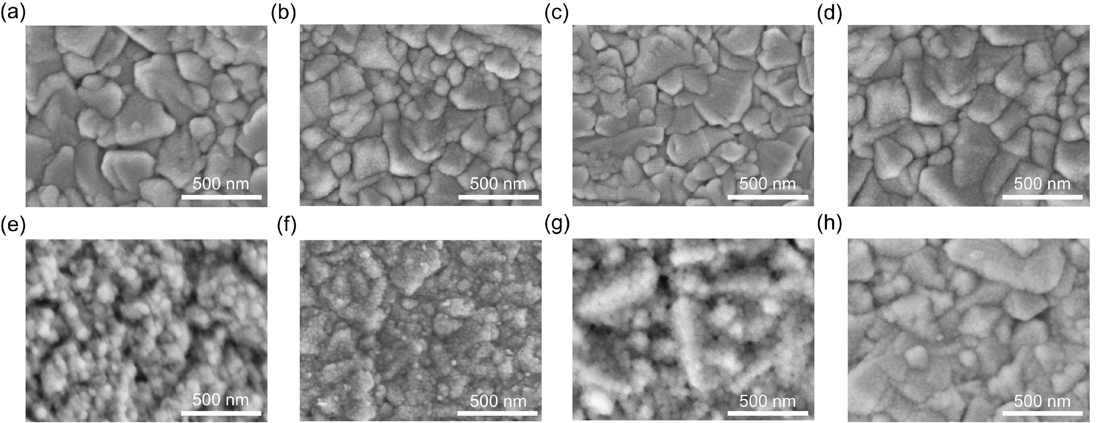
![]() SEM image of sputtered CdS. The first row shows sputtered CdS without ambient air annealing. The second row shows sputtered CdS with CdCl2 spin coating and ambient air annealing posttreatment. The four columns show CdS sputtered at RT, 150 °C, 200 °C and 250 °C from left to right.
SEM image of sputtered CdS. The first row shows sputtered CdS without ambient air annealing. The second row shows sputtered CdS with CdCl2 spin coating and ambient air annealing posttreatment. The four columns show CdS sputtered at RT, 150 °C, 200 °C and 250 °C from left to right.
-
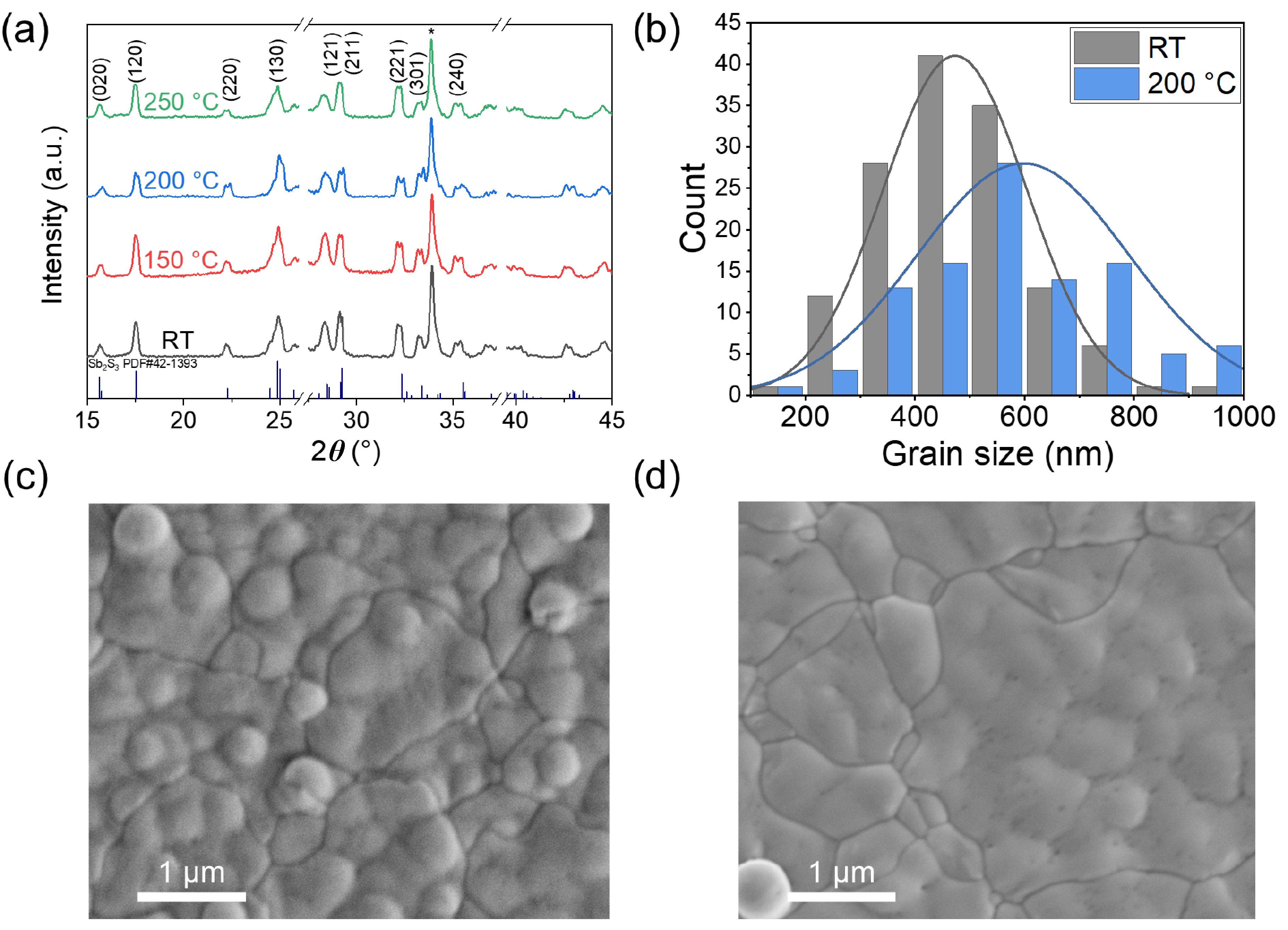
![]() Characterization of Sb2(S,Se)3 thin films grown on sputtered CdS. (a) XRD pattern of the Sb2(S,Se)3 thin film. (b) Statistics on the grain size of the Sb2(S,Se)3 thin film. SEM image of a Sb2(S,Se)3 thin film (c) grown on RT-sputtered CdS and (d) grown on 200 °C-sputtered CdS.
Characterization of Sb2(S,Se)3 thin films grown on sputtered CdS. (a) XRD pattern of the Sb2(S,Se)3 thin film. (b) Statistics on the grain size of the Sb2(S,Se)3 thin film. SEM image of a Sb2(S,Se)3 thin film (c) grown on RT-sputtered CdS and (d) grown on 200 °C-sputtered CdS.
-
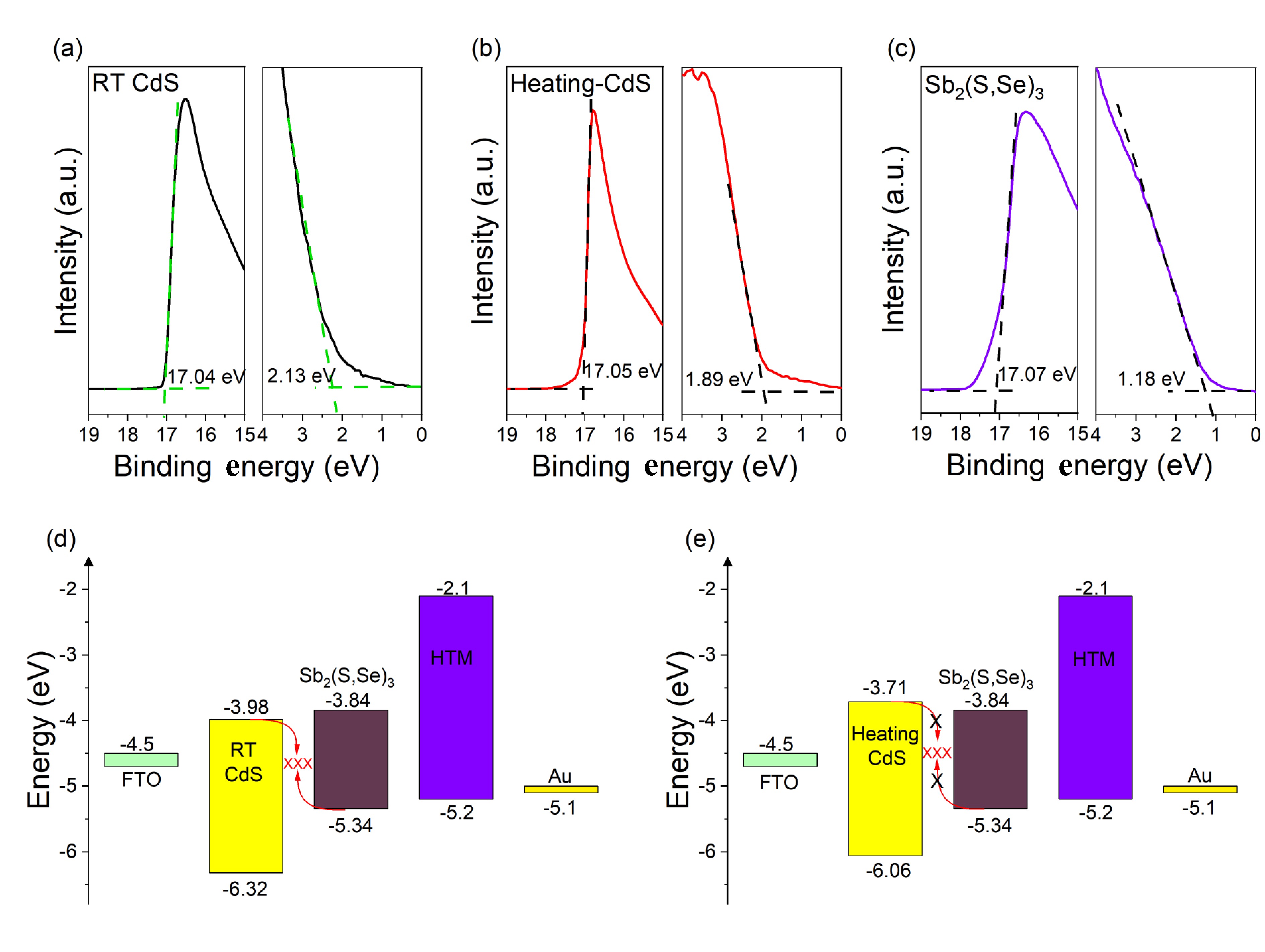
![]() UPS spectra of (a) RT-sputtered CdS, (b) substrate heat-sputtered CdS and (c) Sb2(S,Se)3 thin films. (d, e) Band alignment diagram of the Sb2(S,Se)3 solar cell devices.
UPS spectra of (a) RT-sputtered CdS, (b) substrate heat-sputtered CdS and (c) Sb2(S,Se)3 thin films. (d, e) Band alignment diagram of the Sb2(S,Se)3 solar cell devices.
-
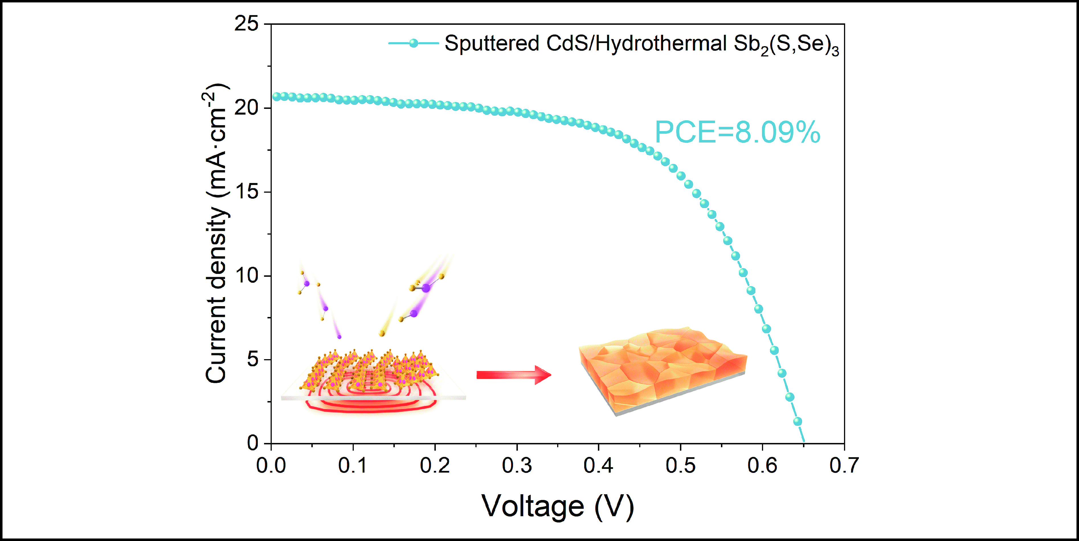
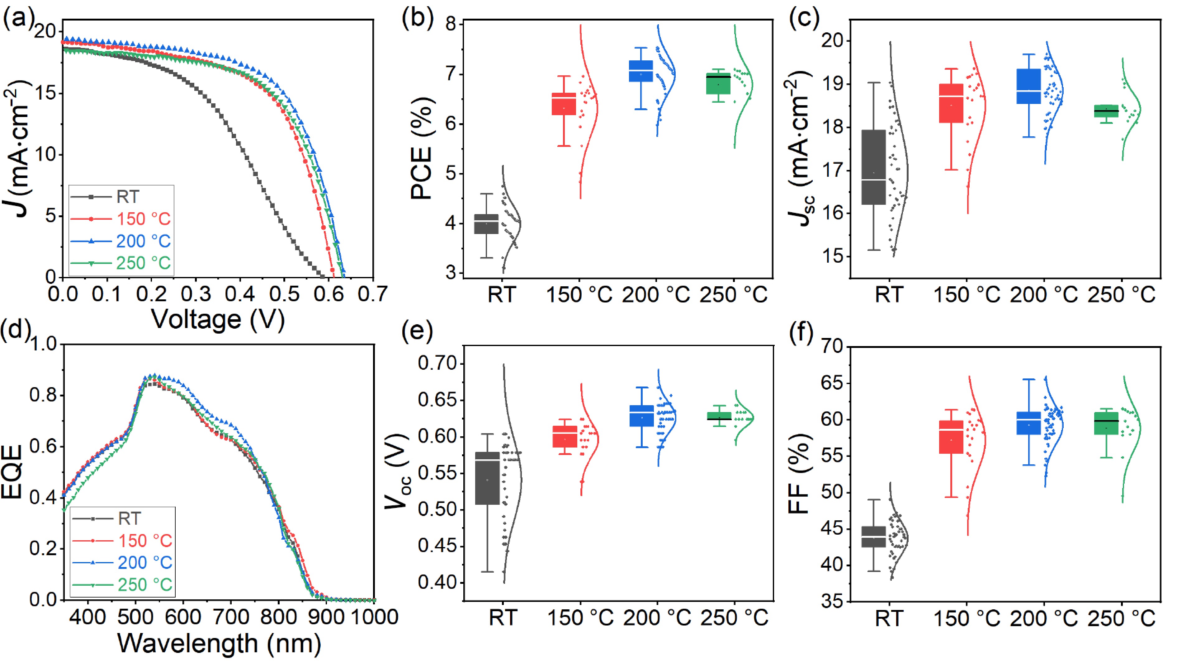
![]() Photovoltaic performance of the devices. (a) Current density–voltage (J–V) curves of Sb2(S,Se)3 solar cell devices grown on sputtered CdS under different substrate heating conditions. Statistical boxplots of the photovoltaic parameters (b) power conversion efficiency (PCE), (c) short-circuit current density (JSC), (e) open-circuit voltage (VOC), and (f) fill factor (FF) of the corresponding devices. (d) External quantum efficiency (EQE) spectra of the corresponding devices.
Photovoltaic performance of the devices. (a) Current density–voltage (J–V) curves of Sb2(S,Se)3 solar cell devices grown on sputtered CdS under different substrate heating conditions. Statistical boxplots of the photovoltaic parameters (b) power conversion efficiency (PCE), (c) short-circuit current density (JSC), (e) open-circuit voltage (VOC), and (f) fill factor (FF) of the corresponding devices. (d) External quantum efficiency (EQE) spectra of the corresponding devices.
-
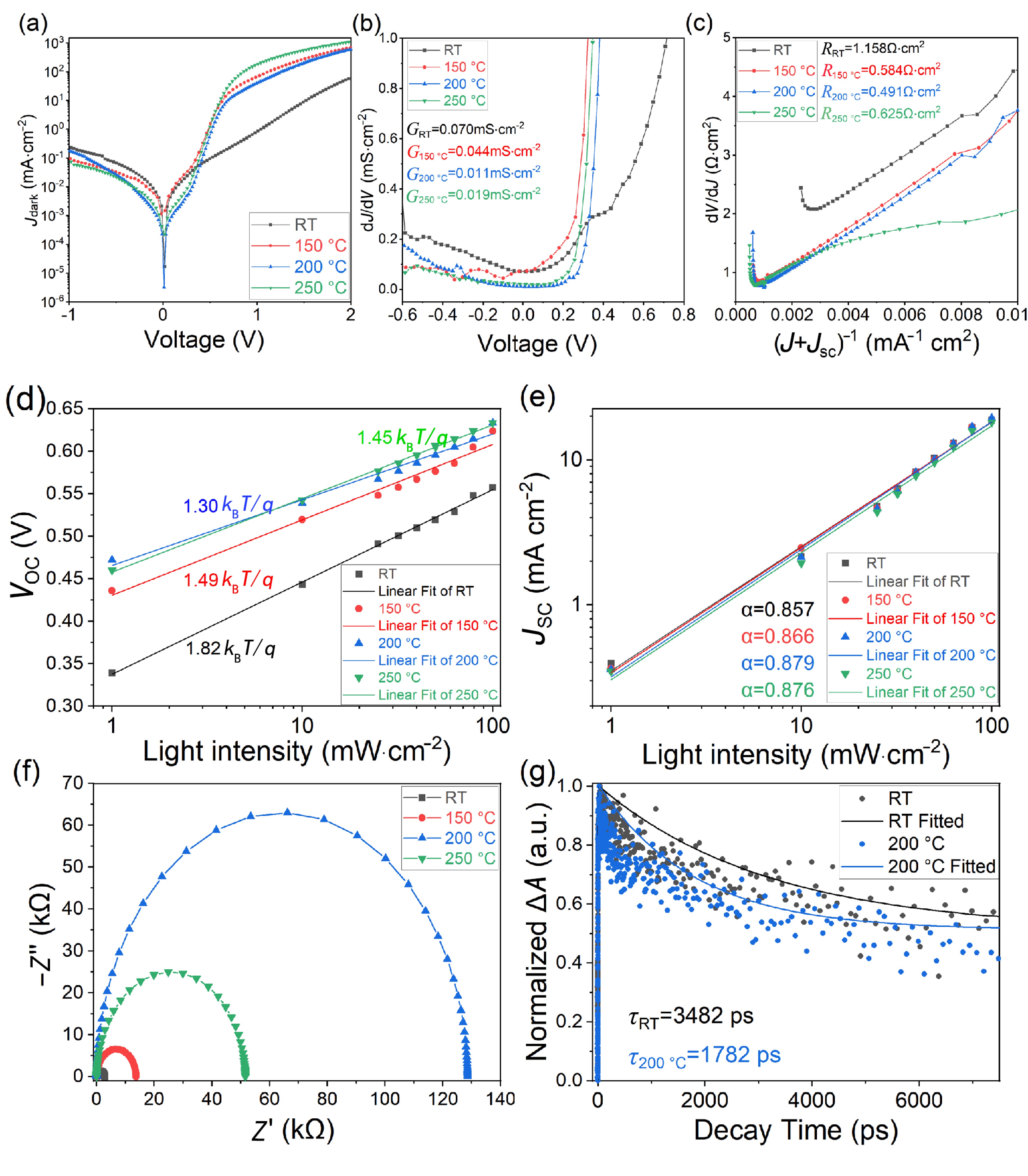
![]() Characterization of Sb2(S,Se)3 solar cell devices grown on sputtered CdS under different substrate heating conditions. Dark current results are shown in the first row with (a) J–V curve, (b) dJ/dV versus voltage plot, and (c) dV/dJ versus (J+JSC)−1 plot. Here, the dark J–V data were measured starting at +3 V, so that (J+JSC)−1 increased to approximately 0.002 mA−1·cm2. Under very high voltage conditions, the derivative increases, forming a tail at the end of the curve. However, this does not influence the analysis by using the well-defined linear part of the curve. The light intensity, electrochemical characterization and carrier transport kinetics of the devices are shown next. (d) Relation between VOC and the logarithm of the incident light intensity. (e) Relation between JSC and the incident light intensity. (f) Nyquist plots (under dark conditions at −0.60 V) of the devices. (g) Original data and fitted curves of transient decay kinetics monitored at 665 nm for Sb2(S,Se)3 films grown on sputtered CdS at RT and at 200 °C.
Characterization of Sb2(S,Se)3 solar cell devices grown on sputtered CdS under different substrate heating conditions. Dark current results are shown in the first row with (a) J–V curve, (b) dJ/dV versus voltage plot, and (c) dV/dJ versus (J+JSC)−1 plot. Here, the dark J–V data were measured starting at +3 V, so that (J+JSC)−1 increased to approximately 0.002 mA−1·cm2. Under very high voltage conditions, the derivative increases, forming a tail at the end of the curve. However, this does not influence the analysis by using the well-defined linear part of the curve. The light intensity, electrochemical characterization and carrier transport kinetics of the devices are shown next. (d) Relation between VOC and the logarithm of the incident light intensity. (e) Relation between JSC and the incident light intensity. (f) Nyquist plots (under dark conditions at −0.60 V) of the devices. (g) Original data and fitted curves of transient decay kinetics monitored at 665 nm for Sb2(S,Se)3 films grown on sputtered CdS at RT and at 200 °C.
-
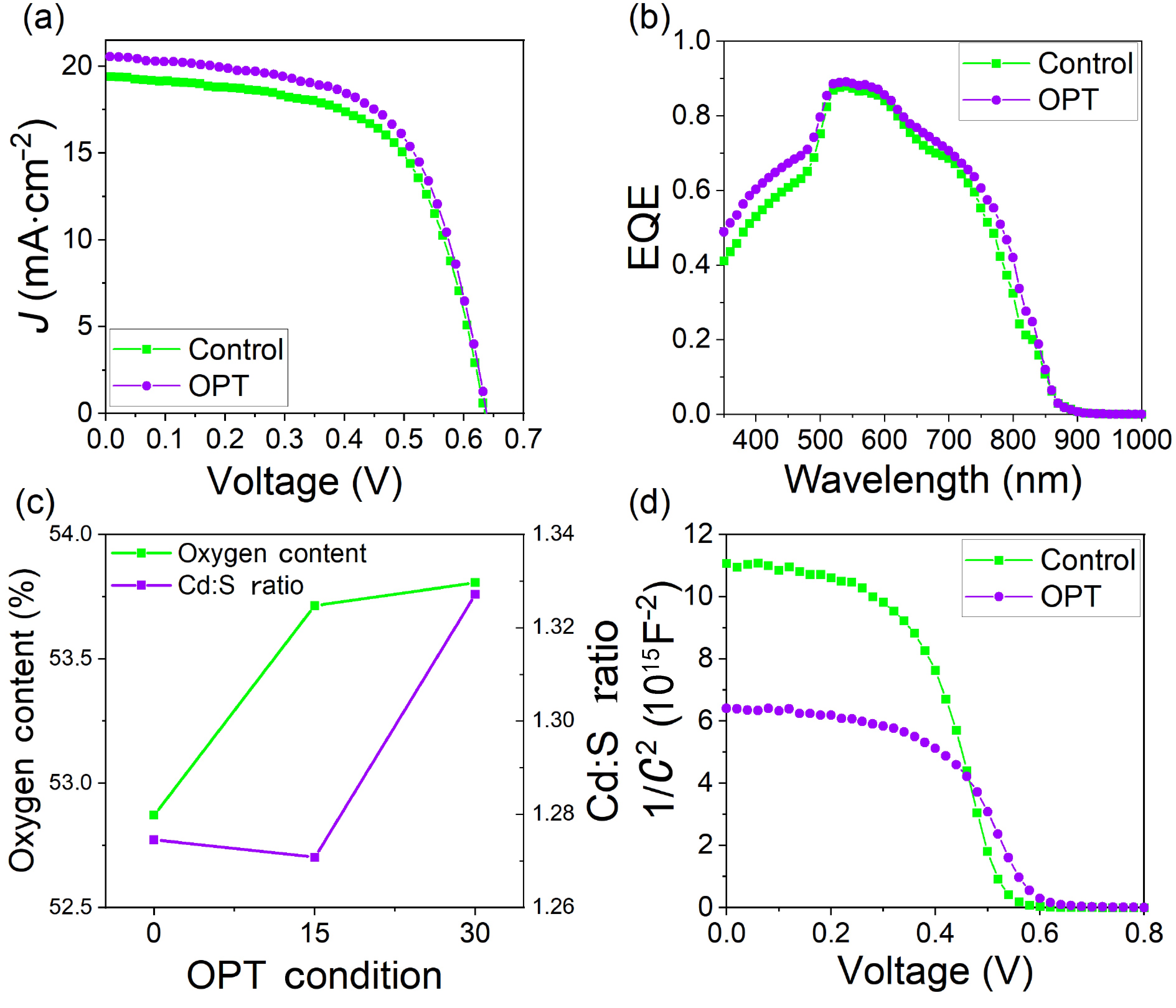
![]() Characterization related to oxygen plasma treatment of sputtered CdS. (a) Full-wavelength EQE spectra of devices with (15 min) and without oxygen plasma treatment (OPT). (b) Champion device efficiency with and without oxygen plasma treatment. (c) Oxygen content and Cd∶S ratio under different oxygen plasma treatment conditions. The results are based on EDS data. (d) The 1/C2–V curves of the devices recorded at a frequency of 100 kHz at RT in the dark.
Characterization related to oxygen plasma treatment of sputtered CdS. (a) Full-wavelength EQE spectra of devices with (15 min) and without oxygen plasma treatment (OPT). (b) Champion device efficiency with and without oxygen plasma treatment. (c) Oxygen content and Cd∶S ratio under different oxygen plasma treatment conditions. The results are based on EDS data. (d) The 1/C2–V curves of the devices recorded at a frequency of 100 kHz at RT in the dark.
Related articles
-
2022, 52(10): 2-1-2-9. DOI: 10.52396/JUSTC-2022-0047
-
2020, 50(11): 1383. DOI: 10.3969/j.issn.0253-2778.2020.11.002
-
2020, 50(6): 733-737. DOI: 10.3969/j.issn.0253-2778.2020.06.003
-
2020, 50(4): 450-456. DOI: 10.3969/j.issn.0253-2778.2020.04.009
-
2017, 47(7): 621-626. DOI: 10.3969/j.issn.0253-2778.2017.07.010
-
2014, 44(8): 623-636. DOI: 10.3969/j.issn.0253-2778.2014.08.001
-
2014, 44(4): 278-284. DOI: 10.3969/j.issn.0253-2778.2014.04.004
-
2010, 40(7): 718-726. DOI: 10.3969/j.issn.0253-2778.2010.07.010
-
2010, 40(4): 363-368. DOI: 10.3969/j.issn.0253-2778.2010.04.006
-
2009, 39(1): 43-49.
